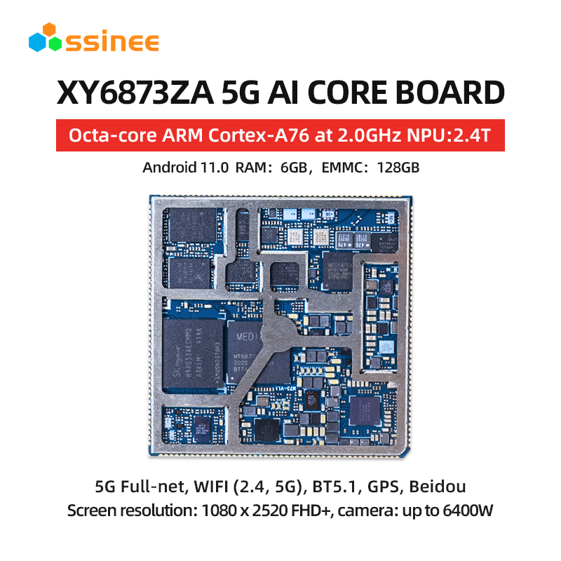
CPU: MediaTek MT6873 Dimensity 720
Architecture: 4X ARM Cortex-A76 up to 2.0GHz + 4X ARM Cortex-A55 up to 2.0GHz
OS : Andriod 11.0
Memory : 4GB+64GB/6GB+128GB
Display : FHD+ support (1080X2520)
Camera : 64 million
Network support : 2G/3G/4G/5G full network access
Wireless connectivity: WiFi/Bluetooth/GPS/Beidou
NPU: 1T computing power
Product introduction
XY6873 is a 5G AI smart module based on MTK’s MT6873 (MediaTek Dimensity 800) platform, industrial-grade high-performance, running Android 11.0 operating system, supporting NR-SA/NR-NSA/LTE-FDD(CAT-18)/LTE-TDD(CAT-18)/WCDMA/TD-SCDMA/EVDO/CDMA/GSM, etc. SCDMA/EVDO/CDMA/GSM etc.; support WiFi 5 802.11 a/b/g/n/ac, BT v2.1+EDR, 3.0+HS,v4.1+HS,V5.1, support Beidou(BeiDou),Galileo,Glonass,GPS,QZSS multiple system satellite positioning; have multiple Audio and video input and output interfaces and rich GPIO interfaces. The supported frequency bands are listed below:
Network band
| Type | Network band |
| NR-SA | N1/N41/N78/N79 |
| NR-NSR | N78+B1/B3/B5/B8,N79+B3/B39,N41+B3/B39 |
| LTE-FDD | B1/B2/B3/B5/B7/B8 |
| LTE-TDD | B34/B38/B39/B40/B41 |
| WCDMA | B1/B2/B5/B8 |
| TD-SCDMA | B34/B39 |
| EVDO/CDMA | BC0 |
| GSM | B2/B3/B5/B8 |
| DL CCA | B1/B3/B7/B38/B39/B40/B41 |
| DL NCCA | B3/B40/B41 |
| Inter CA | B1+B3 B3+B5 B1+B5 B39+B41 |
| UL CCA | B3/B38/B39/B40/B41 |
| WiFi 802.11a/b/g/n/ac | 2400~2483.5MHz/5725~5850MHz/5925MHz |
| BT V2.1+EDR,3.0+HS,V4.2+HS,BT5.1 | 2400~2483.5MHz |
| GNSS | Beidou,Galileo,Glonass,GPS,QZSS |
*Note: The frequency band is subject to specific shipment.
XY6873 is a chip module with 184LCC+237LGA pins. With a size of only 50.0mm × 50.0mm × 2.65mm, it can be embedded in various M2M product applications via solder pads and is ideal for developing mobile devices such as car computers, multimedia terminals, smart homes, IoT terminals, etc.
Remark
1.1. DL CCA: Downlink Intra-band Contiguous Carrier Aggregation
2. DL NCCA: Downlink Intra-band No-Contiguous Carrier Aggregation Downlink Intra-band Non-Contiguous Carrier Aggregation
3. Inter CA: Inter band Carrier Aggregation Inter-band Carrier Aggregation
4.UL CCA: Uplink Intra-band Contiguous Carrier Aggregation Uplink Intra-band Contiguous Carrier Aggregation
Main performance parameters
| Process | 7nm |
| Application Processors | 4xCortex-A76up to 2.0GHz + 4xCortex-A55 up to 2.0GHz |
| GPU | ARM NATT MC4 |
| Camera interface | 4xMIPI CSI(4 Data lanes)64MP @ 30fps |
| video decode | 4K 30fps H.264/H.265/VP9 |
| video encode | 4K 30fps H.264/H.265 |
| LCM interface | MIPI DSI (4 Data lanes) highest resolution support FHD+ (1080×2520) |
| AI Accelerator | Up to 2.4TOPs (2.4 trillion operations per second) |
| Performance | Description |
Modem Processor | 2 MDSP RVSS Processor ARM Maximum Frequency 416MHz |
| Electricity supply | VBAT supply voltage range: 3.5V~4.35V Typical supply voltage: 4.2V |
| Transmitting power | Class 4 (33dBm±2Db) for GSM850/GSM900 Class 1 (30dBm±2Db) for DCS1800/PCS1900Class E2 (27dBm±3Db) for EGSM900/GSM850 8PSK Class E2 (26dBm±3Db) for DCS1800/PCS1900 8PSKClass 3 (24dBm+1/-3Db) for WCDMA bands Class 3 (24dBm+1/-3Db) for CDMA BC0Class 3 (24dBm+1/-3Db) for TD-SCDMA B34/B39 Class 3 (23dBm ±2.7Db) for LTE FDD bands Class 3 (23dBm ±2.7Db) for LTE TDD bands Class 3 (23dBm ±2.7Db) for NR SA bandsClass 3 (23dBm ±2.7Db) for NR NSA bands |
| NR Characteristics | Support 3GPP R15 3.5Gbps DL/775Mbps UL Support 5 – 100 MHz RF bandwidth Support downlink 4 x 4 MIMO,uplink 2 x 2 MIMO SA: Max 2.3Gbps (DL), 625Mbps (UL)NSA: Max 3.5Gbps (DL), 775Mbps (UL) |
| LTE Features | Support 3GPP R11 LTE CAT-18 DL/CAT-13 UL support 1.4 – 20 MHz RF bandwidth support downlink 4 x 4 MIMOFDD: Max 1.2Gbps (DL), 150Mbps (UL) TDD: Max 1.2Gbps (DL), 150Mbps (UL) |
| WCDMA Features | Support 3GPP R9 DC-HSPA+ supports 16-QAM, 64-QAM and QPSK modulation 3GPP R6 HSUPA: 11.5Mbps max (UL) 3GPP R8 DC-HSPA+: 42.2Mbps max (DL) |
| TD-SCDMA Features | Support 3GPP R8 1.28 TDD TD-HSDPA:MAX 2.8Mbps(DL) |
| GSM/GPRS/EDGE Features | EDGE: Support EDGE multi-slot class 12 Support GMSK and 8PSK encoding formats: CS1-4 and MCS 1-9 |
| WLAN Features | 2.4GHz/5GHz dual-band, supports 802.11a/b/g/n/ac, up to 1700Mbps, supports AP mode |
| Bluetooth Features | BT v2.1+EDR,3.0+HS,v4.1+HS,V5.1 (Low Energy) |
| Satellite positioning | Beidou,Galileo,Glonass,GPS,QZSS |
| EMMC/UFS | Supports up to UFS2.1, 256G Byte. |
| DDR | Supports up to 12G Byte @ 2 channels 16bit x LPDDR4X 4266MHz |
| SMS | Text with PDU mode point-to-point MO and MT SMS Broadcast SMS storage: default SIM |
| AT command | Not supported |
| Audio Interface | Audio input: 3 groups of analog microphone input 1 as a headset MIC input, the other two are normal call noise reduction MIC Audio output: AB class stereo headphone output AB class differential earpiece output AB class differential output to external audio amplifier |
| USB Interface | Support USB3.0 Host/Device mode, data transfer rate up to 5.0Gbps for software debugging and software upgrade, etc. Support USB2.0 OTG |
| USIM card interface | 2 groups of USIM card interface support USIM/SIM card: 1.8V and 3V support dual card dual standby |
| SDIO Interface | Support SD/SDHC/MS/MSPRO/MMC/SDIO2.0 or 3.0 4bit SDIO, 8bit SDIO support hot-swap |
| I2C Interface | 10 I2C groups, up to 400K, up to 3.4Mbps when using DMA with I2C for peripherals such as TP, Camera, Sensor, etc. |
| SPI Interface | 8 SPI interfaces, up to 27Mbit/s, DMA mode supported. |
| DPI Interface | 1 group 12 bit DPI interface, DPI clock up to 148.5MHz. |
| ADC Interface | Quad for general purpose 12 bit ADC,Input range=0.05~1.45V |
| Antenna Interface | 7 RF antenna, WIFI/GNSS/BT antenna, WIFI2 antenna, FM RX antenna interfaces |
| Physical Characteristics | Size: 50±0.15×50±0.15×2.65±0.2 mm |
| Interface: 184LCC+237LGA Warpage: <0.3mm Weight: 10.9g | |
| Temperature range | Normal operating temperature: -20°C to +70°C Extreme operating temperature: -25°C and +80°C 1) Storage temperature: -40°C to +85°C |
| Software Upgrade | via USB |
| RoHS | RoHS compliant |
1. indicates that when the module operates in this temperature range, the RF performance may deviate from the specification, for example, the frequency error or phase error will increase, but it will not drop out.
2. “*” indicates that this feature is currently under development.
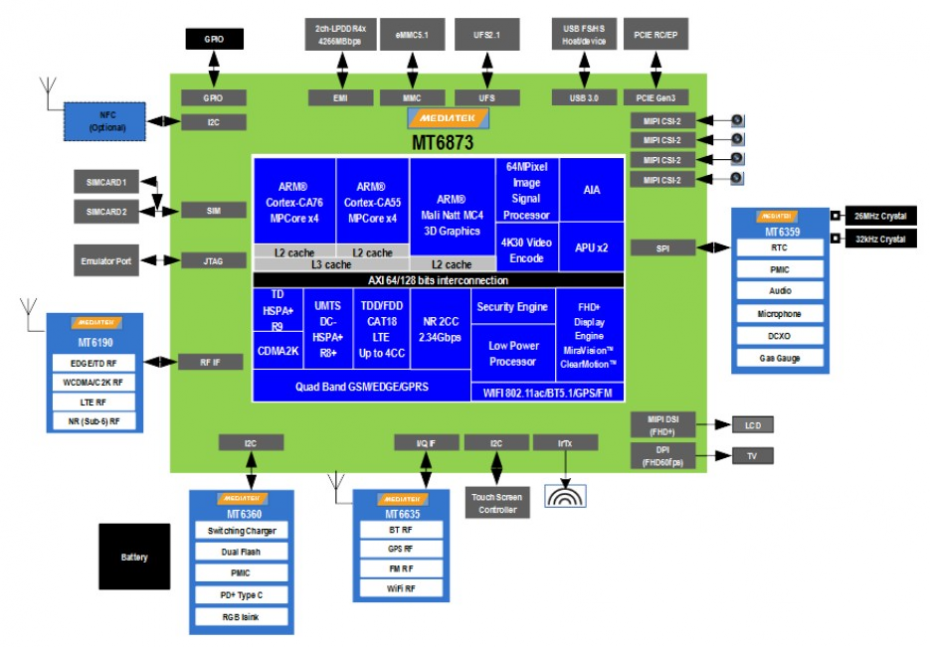
Functional block diagram
The following diagram shows the XY6873 functional block diagram, which describes its main functions:
Power Management
RF section
Baseband section
LPDDR4X+EMMC Memory
Peripheral Interface
–USB Interface
–USIM card Interface
–SDIO Interface
–I2C Interface
–SPI Interface
–ADC Interface
–LCD(MIPI) Interface
–TP Interface
–CAM(MIPI) Interface
–AUDIO Interface

